Loading...
Houston, TX, USA
Mon - Fri : 09.00 AM - 04.00 PM
+1 786 630 29 64
Back to Projects
Completed Project

FPGA-Based Signal
Processing System

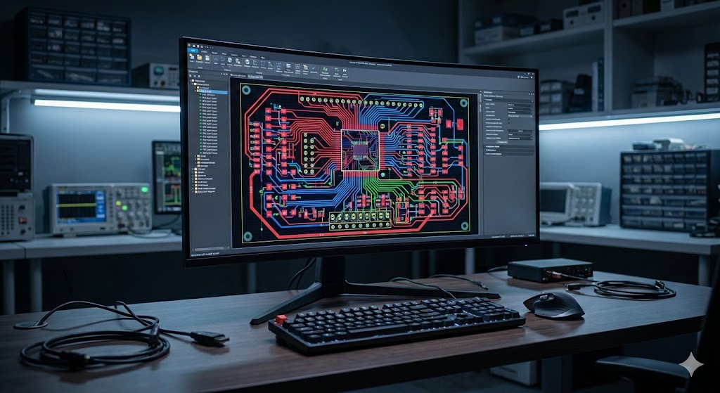
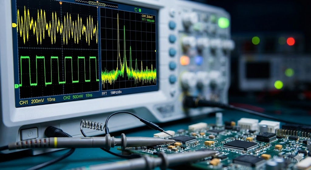
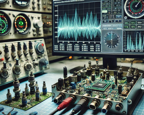
A digital signal processing platform built on a Lattice FPGA. It handles real-time data acquisition, filtering, and spectral analysis at GHz speeds.

FPGA Signal Processing System
2.4
GHz Clock
16
ADC Channels
8
Filter Stages
14
Weeks to Build

System Architecture

Signal Input

A 16-channel ADC frontend with anti-aliasing filters and programmable gain amplifiers

FPGA Core

Lattice ECP5 running pipelined DSP blocks with custom VHDL IP cores

Processing Chain

FIR/IIR filters, FFT engine, and digital downconverter with configurable parameters

Analysis Output

A real-time spectral display with data logging and frequency domain views

Core Capabilities

GHz Processing

A parallel pipeline that reaches 2.4 GHz of effective throughput, with predictable latency under 10 nanoseconds.

Configurable Filters

You can program the FIR and IIR filter coefficients at runtime to set up bandpass, lowpass, highpass, and notch filters.

Real-Time FFT

A hardware-accelerated 4096-point FFT with windowing functions for live spectral analysis and frequency measurement.

Multi-Channel Sync

Phase-locked sampling keeps all 16 ADC channels in step, with synchronization accuracy below one nanosecond.

Deep Memory

A DDR3 buffer holds up to 2GB of continuous signal capture and supports both circular buffer and triggered acquisition modes.

Standard Interfaces

SPI, UART, and Gigabit Ethernet interfaces handle configuration, control, and fast data transfer to host systems.

FPGA Board
FPGA Development Board - Custom Design
PCB Layout
PCB Layout
Signal Analysis
Signal Analysis

Development Process

01
Architecture Design

We specified the DSP pipeline at the system level, analyzed the data flow, and estimated FPGA resource use with Yosys and nextpnr.

02
HDL Development

We wrote custom IP cores in VHDL, including FIR filters, the FFT engine, and ADC interface controllers.

03
PCB Design

A 6-layer PCB with controlled-impedance traces, power integrity analysis, and high-speed signal routing.

04
Simulation & Verification

Behavioral and timing simulation in GHDL and GTKWave, with test benches that cover every operating mode.

05
Hardware Validation

On-board testing with calibrated signal sources to measure SNR, THD, and processing latency.

Project Results

Processing Throughput2.4 GHz
Signal-to-Noise Ratio72 dB
Filter Accuracy99.2%
Power Efficiency3.2W
Channel Isolation85 dB
Tech Stack
Lattice ECP5 VHDL Yosys + nextpnr GHDL + GTKWave KiCad Python SPI DDR3 Gigabit Ethernet GNU Octave Verilog JTAG

Need Custom FPGA Solutions?

From high-speed signal processing to custom digital design, our team builds FPGA-based systems that perform well and run reliably.